Skip to content
Shenzhen, China · Service

High-speed PCB design

Boards other teams turn down: 18 layers, 28,000 pins, and Gen4 links that close on the first fabrication run.

What this solves

  1. The pin count and escape routing consume the layer budget before any high-speed routing starts.

  2. Gen4 and DDR4 links leave almost no margin for skew, and standard serpentine matching introduces its own discontinuities.

  3. Every added layer raises cost and lamination risk, and nobody can say which layer count will actually close the links.

Outcomes

What is different afterwards

Deliverables are the artefacts you receive. These are the things that are true once the work is done.

  1. The layer count is decided by what the links actually need, not by a guess made before routing starts

  2. Every high-speed channel has a simulation result and the budget it was checked against, before release

  3. The stack-up is agreed with the fabricator before fabrication rather than discovered after it

Datasheet

What we have actually shipped

Every figure here is one already delivered on a published project. Check your requirement against it before you write to us.

Max layer count shipped
18
Max pin count on one board
28,400
Max data rate shipped
24 Gbps
Impedance control
100 Ω ±10% differential, agreed pre-release
Via strategy
Back-drilled, stub under 0.15 mm where the budget needs it
Output
Altium or Allegro source, Gerbers, drill and assembly data
Method

How we work on this

What we actually do

We build the stack-up around impedance targets first and let the layer count fall out of that, rather than picking a layer count and hoping the links close. Every high-speed signal layer gets paired reference planes, and no high-speed routing runs adjacent to a split plane.

Density

High pin-count devices spend most of the layer budget on escape routing before a single long trace is placed. The order of work matters: escape strategy and stack-up are settled together, at the start, because discovering the layer count was wrong after placement means starting again.

Timing margin

At 24 Gbps there is almost no room for intra-pair skew. We compensate at the via transition rather than serpentining the trace, which keeps the matched section short and away from the connector field. Back-drilling removes stub resonance on the high-speed vias.

Before release

A layout goes to the fabricator with a DFM review, not over the wall. Stack-up tolerance and back-drill depth are agreed with the people who will actually build it — which is considerably easier when they are half an hour away.
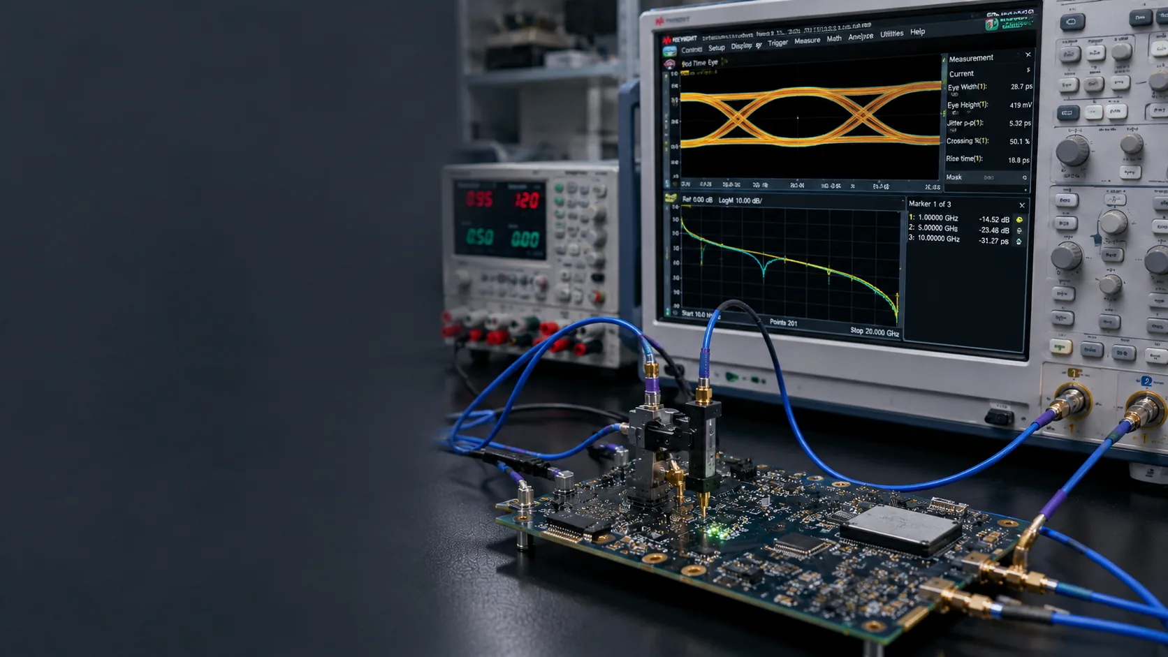
An eye diagram and a network-analyser trace displayed above a board under test
Channel verification before release — the eye at the receiver, against the budget it has to meet.

What you receive

Every engagement ends with a complete handover. The design is yours.

  • Schematic review package at each milestone, not only at the end
  • Stack-up specification built around impedance targets, agreed with the fabricator before release
  • Layout source — Altium or Allegro — plus Gerbers, drill and assembly data
  • Simulation reports for every high-speed channel, with the budget each was checked against
  • BOM with qualified alternates for every part with a single source

Work in this area

1 published
18 layers28,400 pins24 Gbps

Super-computer mainboard

Gen4 PCIe at 24 Gbps across an 18-layer board — first fabrication passed signal integrity sign-off.

Read the case study →
Questions

What buyers ask us first

Answered here rather than on a call, because the answer does not change and your time is worth more than a discovery meeting.

How do you decide the layer count?
The stack-up is built around impedance targets first and the layer count falls out of that. Picking a number first and hoping the links close is how a board comes back needing a respin nobody budgeted for.
Can you work with our existing fabricator?
Yes, and we prefer to. The stack-up tolerance and drill capability are theirs, not ours, and agreeing them before release is what keeps the first fabrication run from being a test run.
Do you simulate, or route and hope?
Every high-speed channel is simulated and the report says which budget it was checked against. Where a channel is marginal we say so while it can still be changed, which is the only point at which the information is worth anything.
Stack-up, 18 layersControlled impedance
L01 SIGL02 GNDL03 SIGL04 GNDL05 SIGL06 PWRL07 PWRL08 GNDL09 SIGL10 SIGL11 GNDL12 PWRL13 PWRL14 GNDL15 SIGL16 GNDL17 SIGL18 SIG100 Ω ±10%FR-4 / low-loss hybrid18 layers · 2.20 mmback-drilled via · stub < 0.15 mm
FR-4 / low-loss hybrid — back-drilled via, stub < 0.15 mm

Platforms we work with

  • DDR2 / DDR3 / DDR4 / DDR5
  • PCIe Gen3 / Gen4
  • SERDES
  • SDI
  • USB 3.x / OTG
  • Ethernet 1G
  • MIPI
  • RS-232 / 422 / 485
  • Altium Designer
  • Cadence Allegro
  • Mentor HyperLynx
  • Keysight ADS

Next step

Send us the hard part.

A schematic, a spec, or a rough idea. We’ll come back within one business day with an honest read on feasibility, risk and timeline.