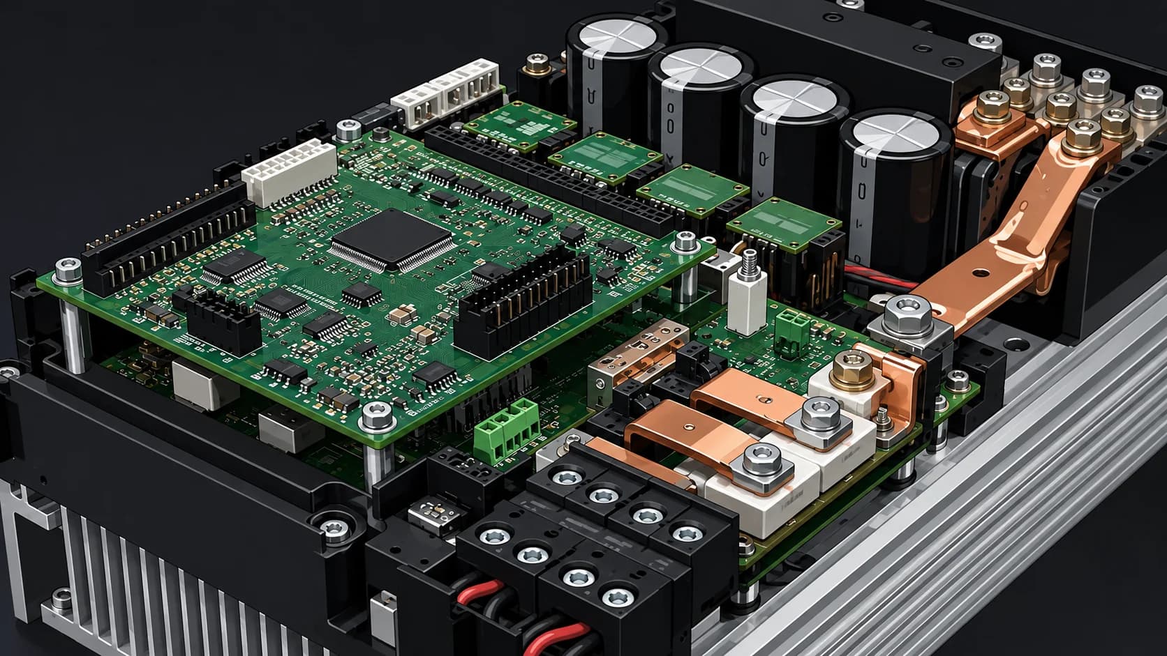
TMS320F28FOC / DTC11 kW
11 kW sensorless AC servo drive
Sensorless field-oriented control at 380 V and 75 A, validated on elevator traction loads from 3.3 to 7.5 kW.
Read the case studyEmbedded firmware, high-speed PCB and FPGA design — from concept to mass production.
We build the boards other teams turn down: 28,000-pin server mainboards, 12 Gbps signal paths, 11 kW servo drives. 200+ designs delivered since 2016, with production support that does not stop at the prototype.
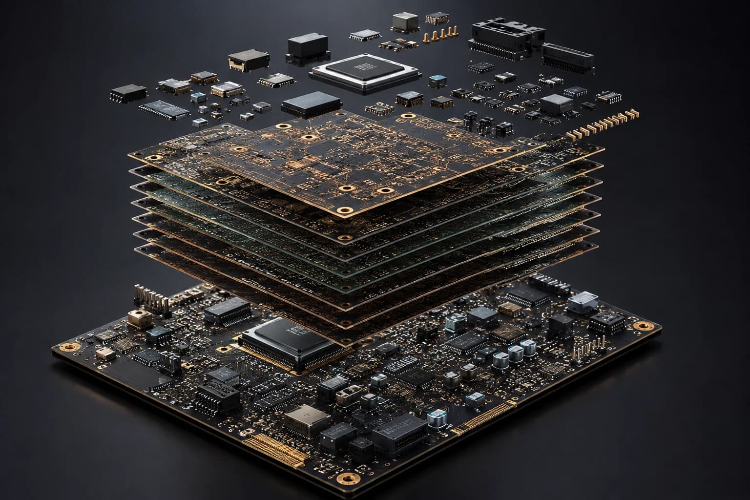
Six capabilities, held deep rather than listed wide. Exhaustive part and platform lists live at the foot of each service page.
Every case follows the same eight-block format — including how the design was proven before fabrication, which is the block most competitors leave out.
Sensorless field-oriented control at 380 V and 75 A, validated on elevator traction loads from 3.3 to 7.5 kW.
Read the case study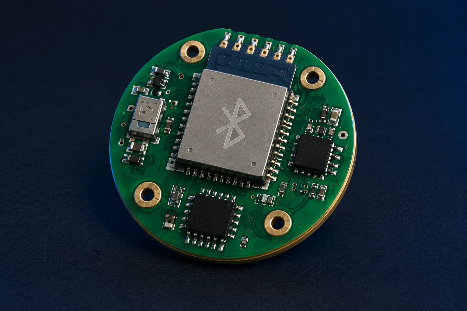
A connected dosing device with flash-backed event logging, native iOS and Android apps, and idle current held below 5 µA.
Read the case study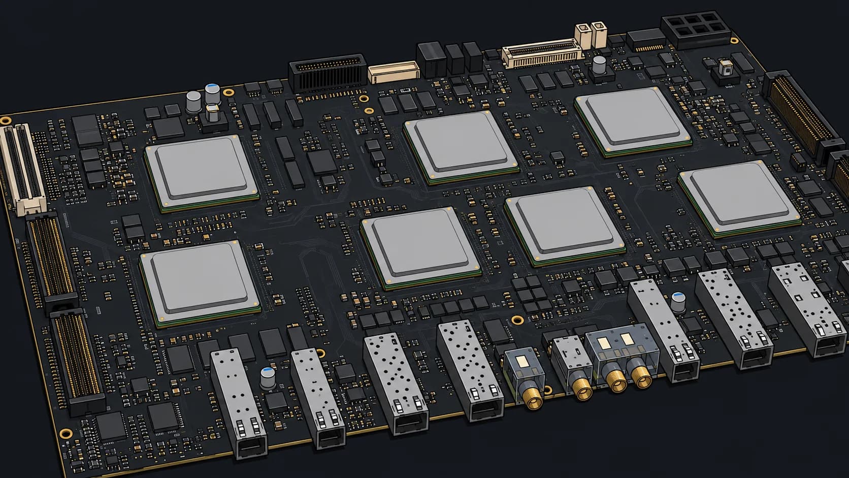
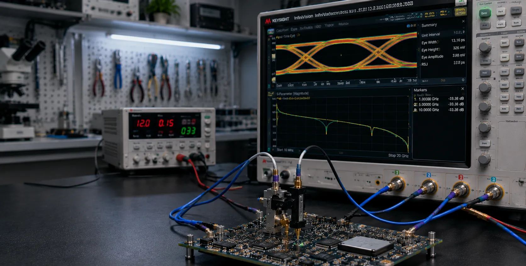
Gen4 PCIe at 24 Gbps across an 18-layer board — first fabrication passed signal integrity sign-off.
Read the case studyEach links to the cases published in that sector.
Six stages, each with a named deliverable. This is the section that answers the real objection to an offshore team: not capability, but process opacity.
Requirements review, feasibility, risk list
Technical proposal and fixed quote
Block diagram, part selection, stack-up plan
Architecture document, BOM v0
Schematic, layout, firmware, RTL
Schematic review package, weekly build
SI/PI simulation, DFM check, design review call
Simulation report, DRC/DFM report
Fabrication, assembly, board bring-up, debug
Working prototype and test report
DFT, test jig, pilot run, supplier qualification
Full design package — you own all files
Every project ends with a complete handover: schematics, layout source, Gerbers, firmware source, BOM with qualified alternates, and test procedures. The design is yours.
We’re not hiding where we are. It’s the reason you should hire us.
PCB fabrication in 48 hours. Components sourced in 3 days. A design revision that takes three weeks in Europe takes us one. When a critical IC goes end-of-life, we walk into the market and qualify an alternate the same week.
We don’t hand you a Gerber file and disappear. We run the DFM review with the fab, build the test jig, sit through the pilot run, and inspect the first production batch — because the factory is thirty minutes from our desks.

Check your requirements against this before you write to us.
Prices are quoted per project, but the structure is not a secret.
Well-defined boards or firmware modules
Scope, deliverables, milestones and price agreed before kickoff. Payment tied to milestone acceptance. Typical 6–16 weeks.
Ongoing product lines and multi-board programs
A named team of 2–6 engineers working in your tooling, your sprint rhythm, your repo. Monthly rate. Minimum 3 months.
A board that won’t pass, a link that won’t close
We audit your existing schematic, layout or firmware and deliver a findings report with a fix plan. Typical 1–3 weeks.
Send a schematic, a spec, or a rough idea. We’ll come back within one business day with an honest read on feasibility, risk, and timeline — before any commitment.