Super-computer mainboard
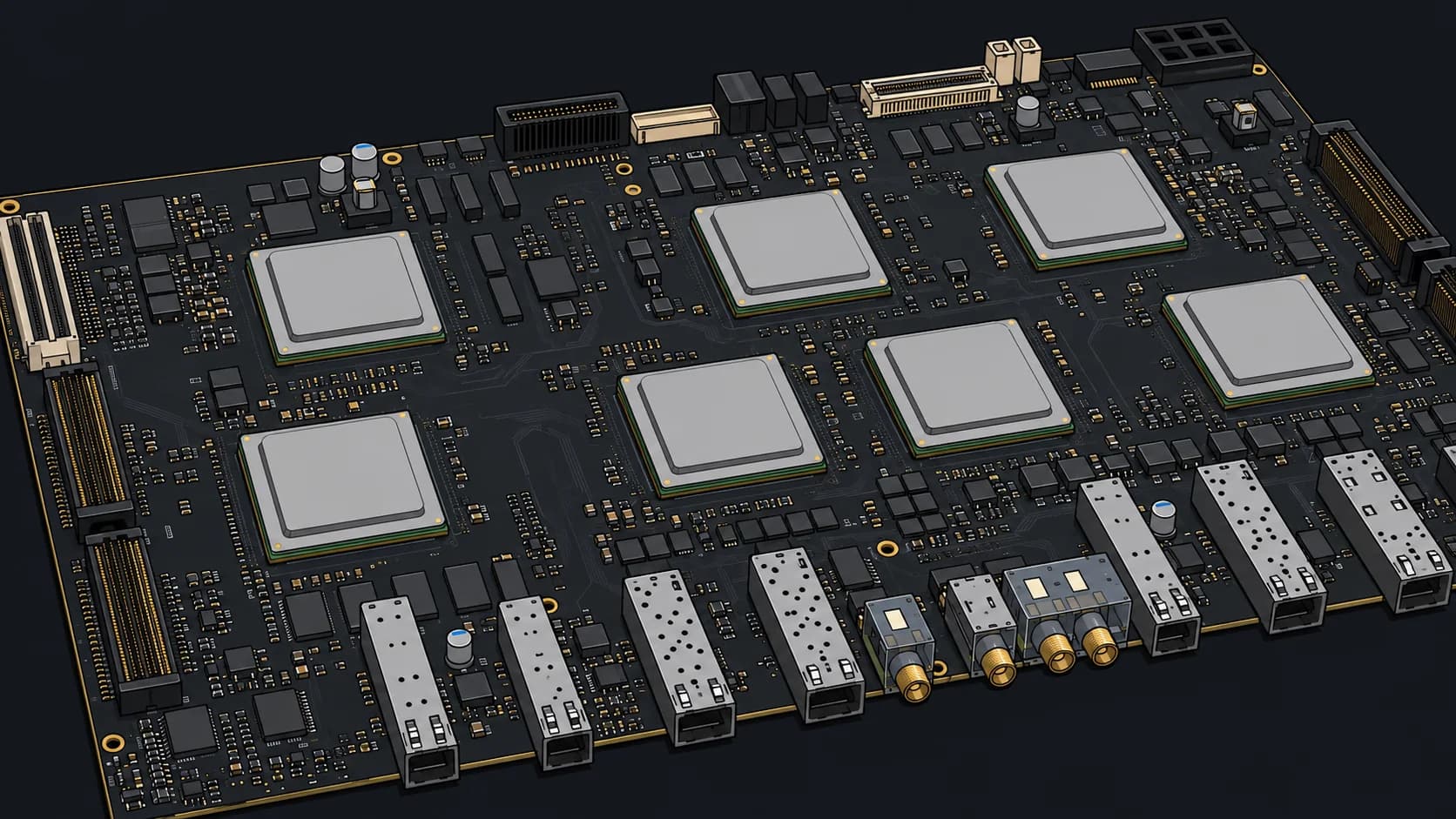
An 18-layer, 28,400-pin server mainboard carrying Gen3 and Gen4 PCIe — designed, simulated and signed off for signal integrity on the first fabrication run.
Published with client permission. Some details are generalized under NDA.
Client and context
A computing hardware manufacturer developing a dual-socket compute node for HPC deployment. Client name withheld under NDA.
The customer had an existing board concept but no in-house team with experience routing Gen4 differential pairs at this density.
The challenge
Density. A 4094-position SP3 processor socket, DDR4 DIMM sockets, M.2 and SC3 modules, plus a BMC subsystem — 28,400 pins on one board. Escape routing alone consumed most of the available layer budget.
Gen4 timing. 24 Gbps links leave almost no margin for propagation-delay skew between the two halves of a differential pair. Standard serpentine length-matching introduces its own discontinuities at this rate.
Stack-up economics. Every added layer raises cost and lamination risk. The customer needed the lowest layer count that would still close the links.
Our approach
- Built the stack-up around impedance targets first, not layer count. Eighteen layers with paired reference planes for every high-speed signal layer, and no high-speed routing adjacent to a split plane.
- For Gen4 escapes, used intra-pair skew compensation at the via transition rather than trace serpentining, keeping the matched section short and away from the connector field.
- Separated the BMC and management network domain from the compute fabric with its own power island, so low-speed switching noise never entered the PCIe reference planes.
- Applied back-drilling on all Gen4 vias to remove stub resonance in the upper frequency band.
Verification
How the design was proven before anything was fabricated.
- S-parameter extraction on all Gen4 channels, checked against the PCIe Gen4 insertion-loss budget.
- Eye-diagram and jitter simulation at the receiver for the worst-case channel.
- Crosstalk modeling on the densest escape region under simultaneous-switching conditions.
- PDN impedance analysis across the processor power rails, driving decoupling placement.
- Full DFM review with the fabricator on stack-up tolerance and back-drill depth before release.
Results
- Signal integrity sign-off passed on the first fabricated build
- Layer count held at 18
- Complete design package handed over: Altium source, Gerbers, stack-up spec, simulation reports, BOM with qualified alternates
Technology used
- 18-layer stack-up
- 28,400 pins
- 12 Gbps Gen3 PCIe
- 24 Gbps Gen4 PCIe
- AMD SP3 socket (4094-position)
- AST2500 BMC
- XC6SLX25-2FGG484C
- DDR4 DIMM
- M.2 and SC3 modules
- RTL8211E-VB
- Altium Designer
- HyperLynx
Related work
11 kW sensorless AC servo drive
Sensorless field-oriented control at 380 V and 75 A, validated on elevator traction loads from 3.3 to 7.5 kW.
Read the case study →Sub-5 µA BLE sensor node with companion app
A connected dosing device with flash-backed event logging, native iOS and Android apps, and idle current held below 5 µA.
Read the case study →